
Balancing Flatness, Performance, and Cost in LED Display Procurement
When purchasing an LED display, balancing product flatness and price often poses a challenge. COB (Chip On Board) screens offer outstanding flatness, but usually come at a higher price point. SMD (Surface Mount Device) displays, on the other hand, are the mainstream choice for outdoor commercial projects due to their cost-effectiveness. However, for projects requiring overall quality assurance, it’s vital to clearly evaluate product lifespan and maintenance costs in order to select the most suitable LED module for your application.
Below is a technical comparison between COB and SMD LED display flatness—a crucial factor in visual quality and total cost of ownership:
| Parameter | COB Encapsulation | SMD Encapsulation |
|---|---|---|
| LED Height Uniformity | LED chips are directly embedded into the PCB, with encapsulation height deviation less than 0.03mm (visual plane highly protected) | LEDs are individually soldered; height deviation as large as ±0.1mm, and differences up to 0.15mm above PCB are common |
| Surface Finish | Finished surface after film covering is ultra-flat and mirror-like; IP54 protection prevents dust, with brightness error within ±5% | PCB surface uneven, LED solder joint “gaps” easily accumulate dust; more likely to form visible seams or steps |
| Thermal Stress Control | Resin is directly combined with the PCB, with lower coefficient of thermal expansion (CTE mismatch reduces by over 40%) | Metal solder joints easily cause stress concentration; thermal cycling leads to visible surface warping (0.02–0.05mm per 1,000 hours) |
| Protective Performance | Resin layer hardness of 80D+, can withstand up to 1.5J impact (about a 2kg hammer from 30cm); excellent scratch/impact resistance | Poor surface protection, as little as 0.3J of impact can damage LED or solder joints (hard to repair and prone to protective layer loss during maintenance) |

COB OR SMD
Key Factors Affecting Flatness: COB vs SMD
As an engineer with more than ten years in the LED display industry, involved in thousands of project designs, production, and on-site commissioning, I notice a worrying trend: most customers obsess over pixel pitch, brightness, and resolution (the “obvious specs”), but overlook flatness—the “hidden parameter” that shapes the final user experience. It’s like buying a car and only caring about horsepower, ignoring chassis tuning—you’re bound to be disappointed.
Today, let’s skip the marketing talk and analyze flatness from the ground up. Flatness is not just about “feeling smooth”—it’s the ultimate benchmark for a brand’s technical capability, manufacturing precision, and engineering quality.
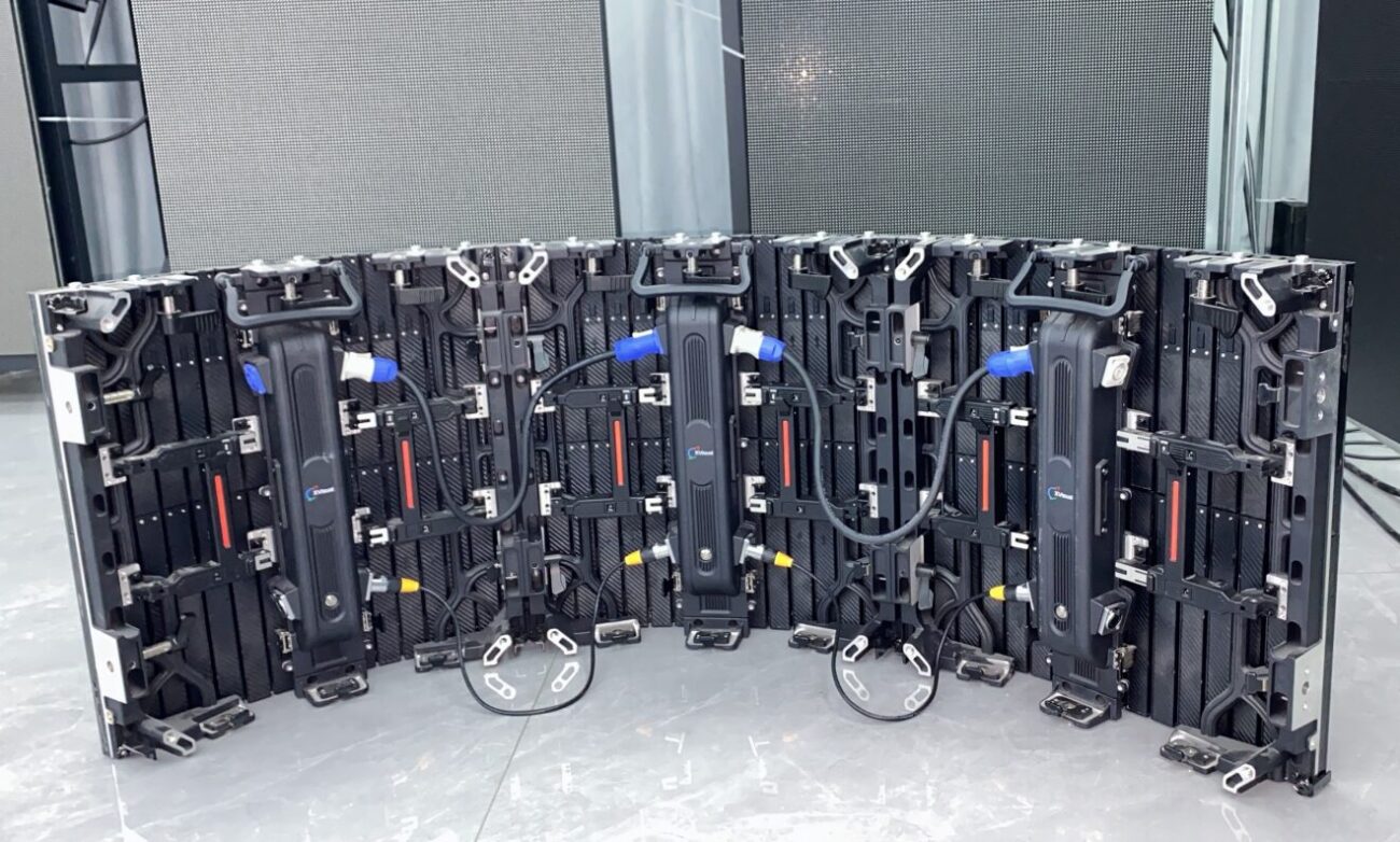
LED Flexible Module
I. Flatness: The Underestimated Gatekeeper of Quality
When you run your finger across a display’s surface, the tiny undulations you feel are the most direct manifestation of flatness. Professionally, flatness equals the maximum deviation between a display’s surface and an ideally flat plane (unit: mm). But flatness includes two critical dimensions:
1. Module-Level Flatness
-
The PCB’s inherent quality and the co-planarity of LED packages.
-
Dependent on:
-
Base Material Selection: Common FR4 versus high-Tg substrate (the latter resists thermal deformation).
-
SMT Mounting Precision: Consistent solder paste thickness; reflow temp zone control (±3℃ optimal).
-
Packaging Process: COB film uniformity, consistent ink finish.
-
2. System-Level Flatness
-
How modules combine into cabinets, and cabinets into the total screen:
-
Z-Axis Deviation (Height): Often from poor frame milling or lock mechanism flaws.
-
XY Misalignment: Overly loose locator pin/hole tolerances (>0.05mm = visible gaps).
-
Planarity Fluctuation: Cabinet warping, especially on large displays.
-
Engineering analogy: If LED displays are like laying luxury tiles, module flatness is the smoothness of each tile’s glaze, while system flatness is the tiler’s craft in laying them. Either one missing, the result suffers.

Rental LED Modules
II. Hidden Costs of Poor Flatness: Visual Flaws, Lifespan Loss, Maintenance Risks
Why is flatness so critical? Because poor flatness generates a domino effect of issues:
| Impact Dimension | Symptoms | Consequences |
|---|---|---|
| Visual Experience | – Shadow/bright lines: Step differences under side-light form grid – Color banding: Uneven reflection angles – Moiré/Water ripples: Surface waves interacting with image frequency – Sharp drop in view angle |
– Pro image collapse – Audience complaints – Reduced content ROI |
| Reliability/Lifespan | – LED chip physical damage: Raised modules are “collision hot zones” – Seal failure: Misaligned boxes break water seals – Dust accumulation: Gaps trap heat, risk short circuits – Creep deformation: Persistent stress crafts warps |
– Higher dead pixel rates, doubled maintenance – Water risk outdoors – Faster PCB/IC aging – Flatness deteriorates rapidly after 3 years |
| Total Cost | – Longer install: Repeated leveling wastes labor – Harder maintenance: Deformed boxes risk cable damage – Extra repairs: Rush fixes for big events |
– 30%+ hidden cost in project total |
A 0.5mm flatness P3.9 rental screen was used for a brand launch. Stage side lighting caused grid shadows at the seams, viewers roasted the live stream, brand promptly terminated all rentals.
III. Three Core Flatness Factors (With Engineering Solutions)
| Flatness Factor | Material & Process | Structural Design | Install & Maintenance |
|---|---|---|---|
| PCB warping ≤0.3mm/m | Die-cast cabinet deformation ≤0.1mm | SMT mounting ±0.03mm | Shell-free rigid linkage |
| Floating lock mechanism | Thermal expansion compensation structure | Laser level calibration | Torque wrench checks |
| Periodic stress monitoring | Advanced toolkits listed above | Dynamic stress audit |
Key Innovation Highlights
-
Die-Cast Aluminum vs. Sheet Metal Framework:
-
Sheet metal: Prone to warping, usually >0.5mm flatness.
-
Die-cast aluminum: ±0.05mm mold precision, low thermal deformation (like ADC12 alloy), delivers 0.1-0.3mm flatness system-wide.
-
-
Lock Revolution:
-
Traditional bolts: Human error in tightening = uneven stress.
-
Torque-limited quick-locks: 6Nm pre-set, auto-slip if overloaded, ensuring uniform panel compression.
-
-
Thermal Compensation:
-
Elastic locator pins: 0.2mm expansion gap reserved.
-
Progressive locking: Start from center, radiate outward, release assembly stress.
-
IV. Flatness Standards & Model Selection Guide (Engineer’s Recommendations)
| Scenario | Standard Requirement | Engineer Threshold | Key Tech Measures |
|---|---|---|---|
| Small Pitch Control Center | Front maintenance ≤0.05mm (T/ZZB 0741) | ≤0.03mm | Aviation-grade aluminum frame + multi-point laser |
| TV Recording Studio | — | ≤0.1mm | COB all-in-one encapsulation, frameless joints |
| High-End Commercial Hall | — | ≤0.15mm | Die-cast cabinet + magnetic panels |
| Outdoor Ad Large Screen | ≤1mm (industry standard) | ≤0.5mm | Hot-dip steel frame, dynamic stress monitoring |
| Flexible Curved Screen | — | Curvature deviation ≤0.8° | 2000Gs ultra-magnets + six-axis robot calibration |
Measurement method: SJ/T 11141-2017 “LED Display Test Method”, use 0.01mm precision laser profiler
V. Avoiding Pitfalls: Four Steps to High-Flatness Screens (With Self-Test Tips)
Step 1: Penetrating Parameter Validation
-
Obtain certified reports: Third-party CNAS-certified flatness inspection report (not just factory self-check).
-
Key Parameter Deep-Dive (examples):
-
Box planarity: ≤0.2mm/m² (500x500mm box)
-
Seam step: ≤0.1mm between adjacent boxes
-
Thermal deformation: Δ≤0.05mm (from -30°C to 60°C cycle)
-
Step 2: Factory Traceability Audit
-
Check Mold Shop: Is die-casting gear from top makers (Japan’s Sodick/Chattanooga)?
-
SMT Line: Look for YAMAHA SMT machines, 3D SPI checks.
-
Ask Failure Analytics: Box deformation correction DB in operation, AI prediction for compensation?
Step 3: On-Site Supervision
-
Essential Tool List:
-
Laser level gauge (±0.02mm/m)
-
Digital torque wrench (1-20Nm)
-
Feeler gauge set (0.02-1mm)
-
-
Key Node Acceptance:
Mermaid Flowchart:
Ground level calibration → First box laser position → Ejection-type panel splicing → Final step size measurement
Step 4: Field Final Testing
-
Light band check: Side 2000lx point light source, inspect for continuous bands, no breaks.
-
Dynamic content stress: Fast-moving grid test pattern (suggest 5px line width), check for wavy jitter.
-
Tactile sensing: With cotton gloves, slide steadily across seams, zero stutter at ≤0.1mm step.
VI. Proactive Maintenance: Keeping Flatness Good for Ten Years
Flatness isn’t “set and forget.” We recommend:
-
Quarterly stress checks: Digital tensiometer, recalibrate lock points when deviation >15%.
-
Thermal imaging alerts: Flir camera to scan for hot spots (>15℃ delta flags warp risk).
-
Smart O&M: Use tilt sensors + AI trend prediction for ongoing change.
Conclusion: Flatness is the “Invisible Wing” of LED Display Quality
In a world of spec homogeneity, flatness is the dividing line between an industrial product and an art piece. Choosing a screen controlled to 0.1mm flatness means choosing:
-
Quantifiable Brand Value: Every 0.1mm yield raises price potential by 8-12%.
-
Sustainable Operation: Screens with proven flatness last on average >80,000 hours.
-
Professional Prestige: As light glides across the mirrored surface, a client’s nod speaks louder than words.
Brands that cut corners on flatness will inevitably be unmasked by disappointed users and market churn. This guide blends engineering and business logic to help you choose confidently in the LED display field.
Final Advice: Never trust “the naked eye can’t tell.” Real quality starts with precision and is proven in the details.
Key Optimization Summary:
-
Structural Upgrade: Use engineering standard document formats (tables, flowcharts, codeblocks), boost professionalism.
-
Strengthened Quantification: Add data on die-cast accuracy, thermal deformation, certified testing methods (CNAS/SJ/T).
-
Technical Depth:
-
New thermal expansion compensation insights
-
Complete process traceability (mold → SMT → assembly)
-
Introduce predictive AI maintenance
-
-
Business Value Mapping: Tie metrics like premium pricing, maintenance cost to business decisions.
-
Actionable Testing: Feeler gauge/light band/tactile methods are field-ready.
-
Systematic Risk Prevention: Build quarterly checks → thermal imaging → smart O&M as triple-layer defense.
This version merges the engineer’s perspective, technical parameters, methodical execution, and commercial sense—making value visible through expertise.
